Scanning electron microscope: More precise in a vacuum
The scanning electron microscope (SEM) is a powerful microscope with which the surface of components can be imaged at high magnification and depth of focus. This makes it possible to examine structures in the micrometre range even on non-polished surfaces, which is not possible with a light microscope.
SEM is often used to analyse fractured components. Based on the microscopic details visible in the fracture surface, it is possible to draw several conclusions about the cause and course of the failure. Among other things, it is usually possible to recognise whether a component is ductile or brittle and from which position the fracture originated. Indications of hydrogen embrittlement, such as gaping grain boundaries and microplasticities on the grain interfaces, can usually also be determined (and can generally only be detected using SEM). SEM analysis is therefore an important factor in determining the cause of fracture.
With its EDX sensor (energy dispersive X-ray spectroscopy), our SEM can also be used to determine and graphically represent the material composition. Examination of corrosion or very thin layers is also part of the field of application.
The functional principle of SEM
The electron source generates an electron beam that is directed at the sample. This beam is moved over the sample in a grid using electromagnets, scanning the area point by point. When the electron beam hits the sample, it interacts with the surface and generates various signals such as secondary electrons, backscattered electrons and X-rays.
The signals generated can be captured with various detectors and converted into images. The information contained in the image depends on the signal used:
- Secondary electron contrast (SE detector): Image of the surface structure
- Backscattered electron contrast (BSE detector): Information about the material density
- X-ray analysis (EDX detector): Determination of the chemical composition
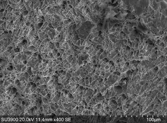
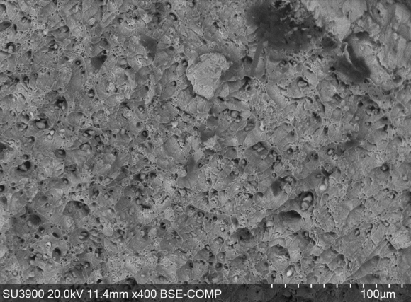
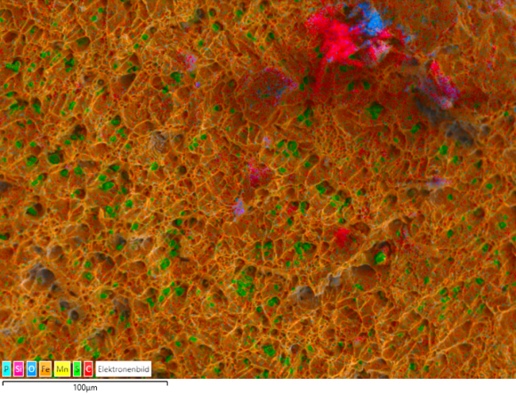
Images of the same sample point with different detectors
The SEM offers a much higher resolution than a light microscope, which means that the smallest details on the surface of the object can be viewed. As the electron beam and the resulting signals are disturbed by air molecules, the examination must take place in a vacuum. The sample should be electrically conductive, but we also have the capability to analyse nonconductive samples.
Your benefits
- Specialised in fasteners
- Several examination options for your testing tasks
- High reaction speed of our laboratory: When components fail, it is also about the speed and flexibility of a testing laboratory. We are your contact in time-critical situations.
The Würth Industrie Service GmbH & Co. KG collects and processes the personal data provided in the form in order to process the requested request for you. Please note the mandatory fields in the forms. The legal basis for this processing, the absolutely necessary data, is Art. 6 para. 1 lit. b DSGVO, implementation of a pre-contractual measure. The processing of data voluntarily provided by you is carried out on the basis of Art. 6 para. 1 lit. f DSGVO. Thereafter, processing is permissible which is necessary to safeguard our legitimate interests. Our legitimate interest is to have contact with you, our customers, to improve our consulting quality and to be able to contact you more easily in case of possible queries. The data collected will only be stored by us for as long as is necessary to process your enquiry and to contact you. They are then deleted.
Supplementary data protection information, in particular regarding your rights to information, correction, deletion, restriction of processing, objection and complaint, can be found in our data protection declaration.